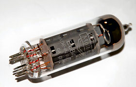
To run integrated circuits at faster and faster speeds, University of Pittsburgh scientists are proposing a new spin on an old method: a change from the use of silicon electronics back to vacuum technology for electron transport – a shift they believe would overcome a significant stumbling block in the ongoing development of faster and more efficient computers.
For the past 40 years, the number of transistors placed on integrated circuits in devices like computers and smartphones has doubled every two years, producing faster and more efficient machines. This doubling effect – known as “Moore’s Law” – occurred thanks to scientists’ ability to continually shrink transistor size, thus producing computer chips with all-around better performance. However, as transistor sizes have approached lower nanometer scales, the laws of physics make integrated circuits increasingly difficult and expensive to build.
“Physical barriers are blocking scientists from achieving more efficient electronics,” said Hong Koo Kim, principal investigator on the project and Bell of Pennsylvania/Bell Atlantic Professor in the University of Pittsburgh’s Swanson School of Engineering. “We worked toward solving that road block by investigating transistors and its predecessor – the vacuum.”
“The best way to avoid this scattering – or traffic jam – would be to use no medium at all, like vacuum or the air in a nanometer scale space,” said Kim. “Think of it as an airplane in the sky creating an unobstructed journey to its destination.”
However, says Kim, conventional vacuum electronic devices require high voltages, and they aren’t compatible with many device applications. Kim and his team decided instead to set out to redesign the structure of the vacuum electronic device altogether.
The researchers discovered that electrons trapped inside a semiconductor at the interface with an oxide or metal layer can be easily extracted out into the air. The electrons harbored at the interface form a “sheet of charges” and Kim found that the Coulombic repulsion (the interaction between electrically charged particles) in the electron layer enables the easy emission of electrons out of the silicon. The team extracted electrons from the silicon structure efficiently by applying a negligible amount of voltage and then placed them in the air, allowing them to travel ballistically in a nanometer-scale channel without any collisions or scattering.
“The emission of this electron system into vacuum channels could enable a new class of low-power, high-speed transistors, and it’s also compatible with current silicon electronics, complementing those electronics by adding new functions that are faster and more energy efficient due to the low voltage,” said Kim. “There is the potential for the vacuum transistor concept to come back, but in a fundamentally different and improved way.”
Related:
Discuss this article in our forum
First inexact computer chip aimed at developing world
Novel material could revolutionize electronics
Nanotronics within reach with creation of molecule-sized diode
Chaos computing researcher touts new silicon “chaogate”








Comments are closed.