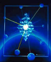
With equipment so sensitive that it can locate clusters of electrons, Cornell University and University of Tokyo physicists are attempting to explain the puzzling behavior in a high-temperature superconductor, perhaps leading to a better understanding of how such superconductors work.
The researchers say that under certain conditions, the electrons in the material pretty much ignore the atoms to which they are supposed to be attached, arranging themselves into a neat pattern that looks like a crystal lattice. The behavior occurs in a phase physicists have called a “pseudogap,” but because the newly discovered arrangement looks like a checkerboard in scanning tunneling microscope (STM) images, researcher J.C. Séamus Davis from Cornell calls the phenomenon a “checkerboard phase.”
Davis, Hidenori Takagi and co-workers describe the observations in the journal Nature. “In at least one cuprate high-temperature superconducting material that phase is an electronic crystal,” Davis reports.
A superconductor is a material capable of conducting electricity with virtually no resistance. Modified crystals of copper oxide, known as cuprates, can become superconductors at temperatures up to about 150 Kelvin when they are doped with other atoms that create “holes” in the crystal structure where electrons would ordinarily be. These superconductors are widely used in industry, although there is still no clear explanation of how they work. Their superconducting behavior begins when about 10 percent of the electrons have been removed, but for over a decade physicists have been puzzled by what happens when somewhat fewer electrons are removed: The material conducts electricity, but just barely. In theory it shouldn’t conduct at all. Davis has now been able to observe this phase with a specially modified STM that measures, in effect, the quantum wave functions of the electrons in a sample.
The Heisenberg uncertainty principle says that we can never tell exactly where an electron is. Rather than thinking of electrons orbiting the nuclei of atoms like little planets, scientists today imagine “clouds” of electrons somewhere in the vicinity. An STM uses a needle so fine that its tip consists of just one atom, scanning across a small surface and measuring current flow between the surface and the tip. Conventional STMs scan with enough precision to image individual atoms. Davis has increased the scanning precision to a point where he can resolve details smaller than atoms. His new instrument is so sensitive that it has been built in a room mounted on heavy concrete pillars and isolated by air springs. For these experiments, it scans a sample and reads the probability that electrons are in certain locations, based on current flow through the STM tip.
Davis’s team studied a copper oxide containing calcium and chlorine that was doped by replacing some of the calcium atoms with sodium to remove, in various samples, from 8 to 12 percent of the electrons. The material was cooled to about 100 milliKelvins, or a hundredth of a degree above absolute zero. What they found was that the electrons in the sample arranged themselves in tiny squares, all in turn arranged in a neat checkerboard pattern. The same pattern was found at the highest level of doping tested, where the material begins to become superconducting. Whether or not it continues at higher levels remains to be seen, Davis says.
Theoretically, Davis says, this arrangement should not conduct electricity at all, because the electrons are locked into their crystal-like pattern. “It’s always been a mystery, how do you get from an insulator through a tiny change to a superconductor,” he notes. “Having empirical knowledge of what this phase is may help us to get from here to there.”







Comments are closed.